


The 2024 Embedded World Exhibition & Conference in Nuremberg, Germany, on 9-11 April, featured a total of 12 MIPI-related presentations—nine within the MIPI I3C, MIPI and Automotive Design tracks, and three additional presentations included in other sessions within the program. MIPI also served as a Community Partner for this year's event.
Read more below about the sessions and download the presentation slides where available.
MIPI I3C Track
Session 5.4 Board Level Hardware Engineering
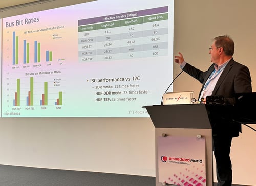
MIPI I3C, The Next-Generation Utility and Control Bus Supporting Time-Critical Applications
Michele Scarlatella (MIPI Alliance)

After an introduction to MIPI I3C®, the presentation focuses on its latest features, including the provision of extra bus lanes that increase the interface speed to nearly 100 Mbps, High Data Rate (HDR) modes that enable improvements in power efficiency and reliability, group addressing that enables multicasting to peripheral devices, and device-to-device tunneling that allows direct communication between target devices. The presentation then focuses on an actual use case and describes how the precise asynchronous and synchronous timing features of I3C provide an efficient framework for data acquisition and control for modern embedded applications. It concludes with an overview of I3C developer resources including the MIPI I3C Host Controller Interface (I3C HCI℠), I3C driver for Linux, conformance test suites, application notes and FAQs.
Demystifying I3C Protocol
Martin Cavallo (Binho)

I3C is becoming more and more popular due to the endless list of advantages it provides over legacy digital communication protocols. However, engineers might still struggle at the very beginning with hands-on experiences. The limited number of ICs on the market supporting the I3C specification, and the lack of examples and application notes from manufacturers commonly lead to confusion, frustration, and a steep learning curve. Prototyping and debugging I3C communication can be hard-going since writing firmware code might be time-consuming, while most protocol decoders and other debugging tools are still limited. Engineers struggle in the early stages of I3C development, with questions such as how the targets' dynamic addresses are managed or how the targets can initiate communication for In-Band Interrupts. Understanding the protocol flexibility based on common command codes -CCC-, the possibility to receive payload with the interrupts, and how the controller behavior relies on the application side can be mind-blowing features for experienced engineers used to dealing with traditional protocols. In this presentation, Binho shares expert insights acquired while working with the I3C protocol. The session aims to demystify the protocol and help engineers overcome all the barriers they might face in their first steps with I3C adoption, showing how to get up and running with the protocol as quickly as possible using hardware and test tools currently available
Benefits of MIPI I3C Through Real World Implementations
Lars Häring (Microchip Technology)

In the rapidly evolving landscape of embedded systems and IoT devices, the choice of communication protocols plays a pivotal role in shaping performance, efficiency and versatility. As technology continues to advance, the need for protocols that can meet the demands of both high-end applications and everyday devices becomes increasingly apparent. While not seeking to supplant established protocols, I3C represents a promising path forward for the future of communication protocols. Applications such as system management, memory access and industrial automation have traditionally used I2C, SPI and USART as serial communication protocols. In this presentation, we demonstrate, through real hardware implementation, how I3C reduces power consumption, simplifies board layout and expedites data transfer rates in such applications. In conclusion, we are demonstrating how the I3C protocol brings practical improvements to serial communication and how it effectively addresses the drawbacks of existing protocols, while retaining and enhancing their benefits making it a reliable choice for a wide range of applications.
MIPI Track
Session 5.5 Board Level Hardware Engineering
Challenges and Solution Supporting HiRes 13+ MP Camera Sensors within MIPI D-PHY Domain
Mark Hoopes (Lattice Semiconductor)
MIPI D-PHY℠ is one of the common LP interfaces for camera sensors connection with Application Processor or SoC. As sensor bandwidth requirement expands the interface must extend to multi-lane, and with ever increasing demand for HiRes the bandwidth supplied by max 4-lane D-PHY is not sufficient to meet 13+ MP @30-60 FPS streaming resolution. Some platforms prefer to stay with exiting IO interfaces like D-PHY to carryover the mechanical and material engineering, or Si SerDes IO availability. For those cases MIPI D-PHY specification does not define interface greater than 4-lane, leaving open for custom implementation. This paper shows an example IO architecture to go beyond 4-lane D-PHY to innovate and support upto 8-lanes. The motivation is to reuse current infrastructure and comply with D-PHY electrical specifications and expand the bandwidth. The interface utilizes single clock lane per pair of 4-data lanes and show a method to deskew data lanes across dual input forwarded clock. This paper list some of the applications of HiRes camera and explains the motivation, challenges, and solution space. The architecture is scalable and configurable to support flexible IO configuration for single HiRes sensor, or multiple traditional 4K cameras. The call for action is for implementers to reduce the risk and adopt 8-lane D-PHY for HiRes camera sensor and benefit from existing success of MIPI D-PHY technology.
MIPI DSI/CSI-2/D-PHY Interface Overview
Ali Osman Ors and John Phillippe (NXP Semiconductors)

This presentation gives attendees a full understanding of the MIPI DSI®, CSI-2® and D-PHY specifications and operations. It starts with a basic explanation of digital images - the relationship between resolution, blanking parameters, frame rates and the pixel clock. Next, it covers how DSI converts this into a serial data stream for transport over a PHY, and how D-PHY works, specifically the differences and transitions between the low speed and high-speed modes. It concludes by covering the CSI-2 interface with a focus on the main differences from the DSI interface.
MIPI CSI-2 - Enabling Machine Vision in Industrial Applications
Ariel Lasry (Qualcomm), Vice Chair of the A-PHY Working Group

MIPI CSI-2 is the most widely implemented embedded camera interface within mobile devices, and its continued evolution has helped deliver major advancements in machine vision and significant economies of scale within the image sensor market. Many adjacent industries beyond mobile now leverage CSI-2 enabled image sensors. This has led MIPI to supplement its core CSI-2 specifications with additional physical (PHY) layer interface options, such as MIPI A-PHY®, which is designed to streamline CSI-2 integration in environments that require longer reach interfaces, such as automotive, industrial and other market sectors. MIPI has also developed a new embedded security framework, targeted initially at machine vision applications. This presentation focuses on the use of CSI-2 to enable machine vision within industrial applications. It explains the PHY options supported by CSI-2 and their applicability for industrial applications. The presentation then works up the MIPI camera "stack" to explain how protocol adaptation layers extend the capabilities of CSI-2 from a short-range, point-to-point interface to a networked interface capable of operating over long-range wired and wireless networks. The remainder of the presentation demonstrates how MIPI Camera Service Extensions (CSE℠) provide supporting end-to-end functional safety and security services to enable safe and secure applications in the most demanding industrial environments.
Automotive Design Track
Session 5.10 Board Level Hardware Engineering
MIPI A-PHY Camera Ingestion for Automotive x86 Architectures
Frederik John and Dr. Stephanie Friederich (Intel Deutschland)

The increasing number of cameras in automotive applications lead to a need for high-speed data links satisfying automotive requirements regarding quality, cost, and electromagnetic compatibility. The MIPI A-PHY link is specifically designed for these kind of long reach, high-speed, automotive applications including built-in safety and security features. The MIPI A-PHY standard brings the advantages of an open SerDes (Serializer/Deserializer) specification into the field of automotive use cases, where 2nd source availability and a broad ecosystem for integration and testing is essential. Providing the MIPI A-PHY technology to the x86 ecosystem is in vital interest for upcoming automotive platforms. In this paper we describe a scalable, modular platform with an Intel 13th Gen Raptor Lake processor. The platform includes a SerDes add-in card, hosting two quad deserializers, to connect eight cameras with full HD CMOS RGGB image sensors over 5m coax cable to the host system. The proof-of-concept shows the implementation of six parallel video streams connected to the MIPI CSI-2 RX ports of the system on Chip (SoC). The raw camera data is processed in the Image Processing Unit (IPU) inside the SoC, utilizing dedicated hardware accelerators for e.g., gain control, white balance, and HDR stitching. The camera streams are routed to a display output to proof that the video pipes are functional. This is the first fully functional enablement of an A-PHY link on a x86 platform.
Connecting the Automotive Future: A Harsh Environment for Moving Bits
Dr. Julien Henaut (BitifEye Test Solutions) and Kevin Kershner (Keysight)

Cars are now massively embedded systems in an environment with wildly varying electromagnetic interference (EMI), temperatures of -40 to +150 C, humidity from frozen to soaked to desiccated, and high-speed collisions, plus they must perform to spec for 20+ years and 300,000+ km. The number of sensors, serdes, and interconnects is increasing exponentially from advanced driver-assistance systems to autonomous vehicles, and I/O rates are approaching 100 TB/day. Automotive interconnects consist of cable segments routed around firewalls, bumpers, and doors, have reflection-generating connectors, and suffer increased loss and shielding deterioration as the years pass. Managing the error rate in this dynamic, safety-critical environment requires highly adaptive, DSP-based serdes that can track channel degradation. The automotive industry is leveraging HSS (High-Speed Serial) technology, like USB and gigabit Ethernet, but signal integrity problems on the street are more challenging than anything in a datacenter. Our presentation addresses the design, diagnostic, and compliance testing methods required to ensure error-free communication links composed of interoperable components through the vehicle lifespan. We show how to emulate the noise spectra and time-profiles specified by the emerging standards—MIPI's A-PHY, Automotive Ethernet, and ASA—and present measurements that demonstrate how DSP-based SerDes can track cable degradation and the extent to which they can cancel EMI.
MIPI A-PHY v2.0 Introduction
Edo Cohen (Valens Semiconductor), Co-Chair of the MIPI A-PHY Working Group

A-PHY (IEEE 2977) is the first industry-standard automotive asymmetric serializer-deserializer (SerDes) physical layer interface targeted at ADAS/ADS and infotainment applications. It’s part of MIPI Automotive SerDes Solutions (MASS), a framework that simplifies the integration of image sensors and displays with functional safety and security features built in. A-PHY offers direct coupling to MIPI CSI-2 image sensors, and MIPI DSI-2 and VESA DP/eDP displays. Since its introduction, MIPI has evolved the interface to ensure it meets the requirements of the most demanding automotive E/E architectures. This presentation covers:
- New A-PHY v2.0, which adds speed gears that double downlink data rate to 32 Gbps and increases uplink data rate to over 1 Gbps.
- A-PHY support for symmetrical 1 Gbps Ethernet sideband data channels alongside high-bandwidth asymmetrical data channels.
- A-PHY’s Narrow Band Interference Cancellation and PHY-level retransmission scheme to ensure maximum link reliability and ultra-low packet error rate.
- A-PHY use in software-defined vehicles and next-generation centralized automotive E/E architectures
- New A-PHY protocol adaptation layers, which add support for Ethernet and SPI interfaces, alongside existing support for CSI-2, DSI-2, VESA eDP/DP, I2C, and GPIO interfaces.
- New Power-over-A-PHY power classes to address new requirements, including the need to support 48-volt operation.
- A-PHY compliance test suite and compliance program
Additional Member Presentations
Session 7.3 Standards - Embedded Vision and Edge AI Standards
How Can Connectivity Innovations Transform Machine Vision Applications in the Industrial Market?
Yaki Sfadya (Valens Semiconductor)

Implementing effective machine vision isn’t as simple as installing high-resolution cameras in a factory. Considerations must be made for how these cameras fit into the system as a whole – how the data is going to be distributed and processed while maintaining low latency. As the market transitions past Camera Link, connectivity for industrial applications has come to be dominated by three technologies: GigE Vision, USB3.0, and CoaxPress 2.0. Each of these technologies offers some key benefit to the market, whether it be longer link distance, lower latency, or higher supported bandwidth. But the industrial market has the potential to vastly improve its connectivity infrastructure for effective machine vision and factory automation. In this presentation, we review the advantages and disadvantages of the currently used technologies. Further, we review other high-performance connectivity technologies that the industry can use to address the growing needs of machine vision in the industrial market. Finally, we outline two new standards - MIPI A-PHY and HDBaseT-USB3 - that can provide system designers a new level of architectural flexibility.
Session 2.12 Wireless 2 - Connectivity Solutions
Software Defined Radars
Edo Cohen (Valens Semiconductor)

With recent advancements in computing, including cutting-edge algorithms that reduce the load on the MCU, centralized processing units are more capable than ever of handling massive amounts of raw sensor data. Yet despite the many advantages of centralized processing, radars used in automotive today include the MCUs integrated within the packages, sending only low bandwidth processed data to a central ECU. This leads to higher cost/power/complexity radars and limits sensor fusion. Realizing centralized processing of raw radar data has two key requirements from the connectivity solution: sufficient downlink bandwidth and a high-speed control interface. Existing connectivity technologies cannot efficiently meet these requirements. With more radars being implemented as OEMs race towards higher levels of autonomous driving, and with the growing need for sensor fusion, OEMs are beginning to reconsider radar architecture in an attempt to centralize processing for raw radar data.In this presentation, I review the main advantages that centralized processing would offer the industry and why the industry has struggled to reach this - including multi-gig bandwidth and a fast SPI interface; and finally I identify some attempts within the industry to achieve centralized processing radars, including one leveraging the MIPI A-PHY connectivity standard.
Session 6.12 Debugging - Systems & Software Engineering
Reducing the Microcontroller Pin Count by Utilizing its I3C Interface for Debugging
Ingo Rohloff (Lauterbach)

When examining the debug interface of a microcontroller device, one of the primary considerations is the number of pins required for its implementation. Each extra pin means extra cost in a production device. So the goal is to use as few pins as possible. The initial step in addressing this issue was to develop debug interfaces that require fewer pins. As an additional measure, most microcontroller devices offer the option to multiplex alternative functions onto the pins associated with debugging. Ideally, the ultimate objective is to avoid the use of any additional pins solely for debugging purposes. This objective can be accomplished by repurposing a functional, non-debug-specific interface for debugging tasks. With the introduction of the new MIPI I3C interface as a successor to the widely adopted I2C interface, an opportunity now exists to attain this goal. I3C boasts sufficient performance and simplicity, making it a suitable candidate for repurposing this interface for debugging purposes. The MIPI Debug Group has embraced this approach and incorporated I3C in the MIPI debug architecture. In this presentation, we showcase the progress already made in enabling the utilization of I3C for debugging. Furthermore, we delve into the prerequisites and challenges associated with repurposing I3C for debugging, particularly in microcontroller applications.